Optimization of N quantification by EDX-STEM in dilute III-V-Sb nitrides.
- Abstract number
- 407
- Presentation Form
- Poster
- DOI
- 10.22443/rms.mmc2023.407
- Corresponding Email
- [email protected]
- Session
- Poster Session One
- Authors
- Verónica Braza (1), Daniel F. Reyes (1), Miguel Lopez-Haro (1), Guillermo Bárcena-González (2), Sara Flores (1), David González (1), teresa Ben (1)
- Affiliations
-
1. Departamento de Ciencia de los Materiales e IM y QI, Universidad de Cádiz
2. Departamento de Ingeniería Informática, Universidad de Cádiz
- Keywords
Dilute nitrides
GaAsSB alloys
EDX-STEM
ζ-factor
- Abstract text
SUMMARY
GaAsSbN alloys with dilute nitrogen contents represent a promising future due to the possibility of combining bandgap and strain engineering with a high degree of versatility. However, determining the N distribution at the nanometre scale with contents below 5% and in the presence of Sb has been an almost insoluble challenge using conventional analytical techniques. In this work, by optimizing all steps of the quantification process, from acquisition conditions to final signal processing, it was possible to characterise GaAsSbN layers with N contents around ~2%. Moreover, comparison of the potential of the ζ-factor method with respect to the classical K-factor ratio method for quantitative analyses was performed.
INTRODUCTION
The addition of small amounts of nitrogen to III-V alloys has attracted the interest of researchers for decades due to their unique properties, such as a large band gap reduction combined with a decrease in lattice parameter. This makes them suitable for developing III-V functional structures combined with In and/or Sb that are lattice-matched to GaAs substrates. However, the growth of dilute nitride nanostructures remains a complex process as the presence of multiple elements can lead to clustering, composition modulation or phase separation so knowledge of the N distribution is key to the success of these devices. However, despite advances in nanoscale compositional characterisation techniques of scanning transmission electron microscopes (STEM), the analysis of alloys containing light elements with very low composition remains a challenge today.
In this work we propose a refined procedure to quantitatively determine the N content in diluted nitride GaAs(Sb)N layers by energy dispersive x-ray (EDX) spectroscopy. The method combines: i) the optimization of the spectra acquisition parameters (voltage, beam current, etc); ii) two step alignment procedure to eliminate sample drift in spectra series, iii) specific background modelling and deconvolution procedure of elements with nearly overlapping edges and iv) estimation of the z factors of the elements for our EDX detector configuration. The potential of the ζ-factor method using the Super-X detector to quantify N were evaluated and compared with the classical Cliff-Lorimer quantization method.
METHOD AND MATERIALS
Several superlattices and QWs of GaAs(Sb)N grown by MBE on GaAs substrates with thicknesses below 10 nm and nominal N and Sb contents of 2-3 and 4-6%, respectively, were analysed. EDX mappings were performed in a Talos F200X STEM microscope taken at 80 and 200 kV with four embedded Bruker detectors using ChemiSTEM technology and processed using Velox® and self-developed software. Two-step alignment procedure were carried out on the spectra mapping series, the first using the normalized cross-correlation algorithm on the ADF image series simultaneously acquired and the second using the Vandewalle algorithm. The correlation coefficients for the ζ-factor method of the elements were previously calculated from reference samples in our experimental conditions operating at 80 and 200 kV. Careful deconvolution of the Sb (438 eV) and N (392 eV) signals were applied using Gaussian functions.
RESULTS AND DISCUSSION
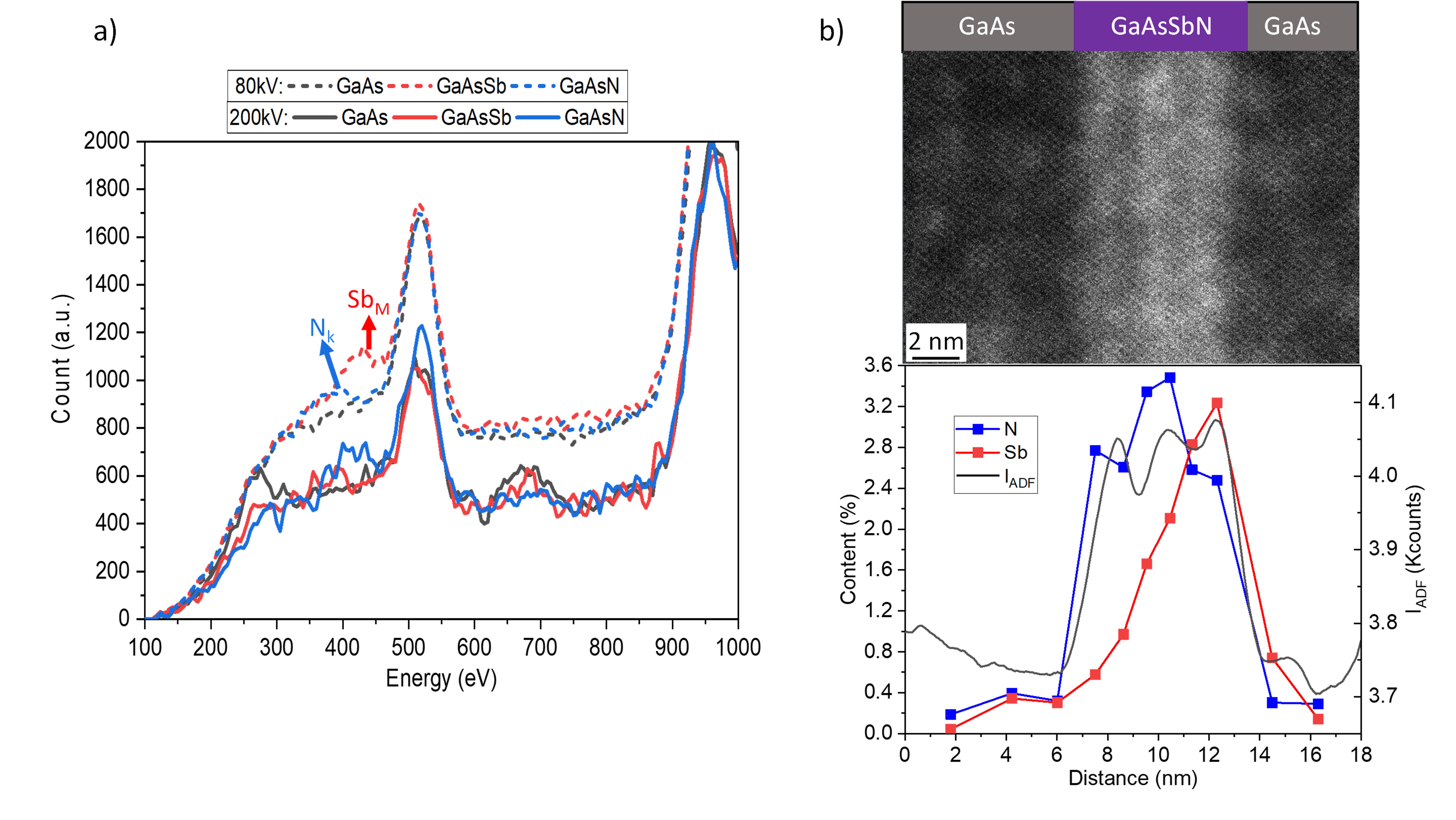
Figure 1.a shows background subtracted EDX spectra of GaAsSb, GaAsN and GaAs regions taken at 80 and 200 kV. As can be seen, the 80 kV spectra show higher signal intensity while the peaks of the higher energy region (not shown here) remain almost unchanged due to the enhanced effective Sb/N cross-section at lower voltages. Furthermore, the additional problem of overlap of Sb and N signals in the case of their simultaneous presence can also be checked helped by the spectra alignment processing. An ADF image of a GaAsSbN quantum well and the resulting average intensity profile along the growth direction are shown in Figure 1.b, where fluctuations in the signal can be seen to exist. Superimposed are the Sb and N composition profiles obtained with our method, where correlation of ADF signal with N distribution is observed. As can be seen, the method allows the N distribution to be quantified at the nanometre level for concentrations below 4%.
Figure 1. a) EDX spectra of GaAsSb, GaAsN and GaAs regions taken at 2 different electron voltages. b) ADF image of a GaAsSbN QW, and in the bottom, its intensity profile along the growth direction. Superposed, the N and Sb average content profiles obtained by applying the proposed methodology in the EDX mapping.
CONCLUSIONS
This work presents a successful procedure for the determination of N profiles with contents below 5% in III-V-Sb semiconductor alloys by EDX spectroscopy. Several steps were necessary to be carried out, from the optimization of the spectral acquisition conditions to the careful alignment of the spectra series, as well as the rigorous signal treatment (background subtraction, signal deconvolution, etc.). The optimized signal was used to assess the possibilities of the ζ-factor quantification method with respect to the traditional Cliff-Lorimer ratio method.