A SPED phase mapping study of electrochemical deposited ceria nanocrystals.
- Abstract number
- 254
- Presentation Form
- Poster
- DOI
- 10.22443/rms.mmc2023.254
- Corresponding Email
- [email protected]
- Session
- Poster Session One
- Authors
- Mr Xuzhao Liu (1)
- Affiliations
-
1. University of Manchester
- Keywords
Precession electron diffraction (PED), phase mapping, ceria catalysts
- Abstract text
Ceria is well known as support material for metal catalysts due to its unique Oxygen Storage Capacity (OSC), which is dominated by the redox pair of Ce3+ and Ce4+. Various characterisation techniques, for example XPS, XAS, XRD and TEM, have been applied to determine the chemical states and crystal structures to understand the relationship between activate sites and possible intermediate states.
However, surface techniques, such as XPS, has large scan area up to hundred microns by hundred microns but have no sensitivity to localised structure. The energy resolution of XPS is limited by the instrument, and for typical lab based XPS, is no better than 0.5 eV. This adds difficulty to distinguish elements in similar chemical structure but different crystal structure. To overcome this, researchers use XAS to study the bonding environment, coordination number of atoms and bonding distance between atoms. As a spectroscopy, it is still hard to link this information with real samples micro or surface structure. DFT simulation of model structures is used to fit the spectroscopy by overlapping each atoms’ simulated peaks together and compare with the experimental data, but still not straightforward. XRD technique is lack of sensitivity to these small particles with no long-range periodic.
Scanning pression electron diffraction (SPED) gives the chance to determine crystal structures, identify lattice parameters and symmetry [1]. In this study, a ceria thin film sample which was firstly studied by in-situ heating XPS and in-situ heating grazing incidence X-ray diffraction (GIXRD) to confirm the chemical states and crystal structure. XPS results indicated the exists of Ce3+ but GIXRD results show only fluorite structure CeO2 exists. Therefore, SPED experiment was carried out on a ceria lamella produced through focused ion beam (FIB) method and conducted using a Talos F200X TEM equipped with Merlin diffraction camera and 10 um C2 aperature.
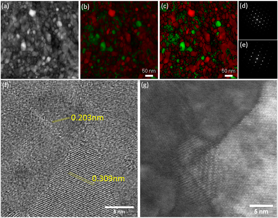
Figure 1. Index map of ceria lamella (a) is generated by NanoMEGAS ASTAR software [2], as well as combined Index/phase/phase reliability mapping (b) and Index/phase/grain boundary mapping. Diffraction patterns (d) and (f) are acquired at positions of two phases (red: CeO2 and green: Ce2O3) with highest reliability: CeO2 (d) and Ce2O3 (e). High-resolution transmission electron microscopy image (f) and high-angle angular dark field image (g) was used to confirm the exists of Ce2O3 nanocrystals.
To reduce ion beam damage and the thickness of the amorphous layer on the side of the lamella, the sample was cleaned use low accelerate voltage and probe current for final cross-section cleaning. HRTEM and STEM-HAADF images were acquired to check the samples’ condition and select the region of interest. Low dose setting with large gun lens and spot size was applied to minimize the electron beam damage induced reduction. SPED data was acquired with precession angle of 0.29 degree, step size of 2 nm and 5 precessions per step to ensure the quality of the diffraction pattern. Index map (Figure 1a) was used as reference image compare with STEM-HAADF image. ASTAR software was used to generate diffraction patterns banks for each phase and index the map for visualization. Phase mapping result (Figure 1b) showed that at least 23.3% of the diffraction patterns are assigned to be trigonal Ce2O3 and the rest should be fluorite CeO2 or CeO2-x, and region where is difficult to match. Due to the overlapping structure and error for matching, the phase reliability for small crystals (a few nanometres) around grain boundaries is lower than the positions in the middle of a big crystal (up to 50 nm). We have to set a threshold 15 of phase reliability to make the matching trustable and this made around 10% mapping region in this 500 nm by 500 nm square can not be trusted. Another reason may introduce difficulty for phase mapping is the intrinsic redox property for ceria. Although electron diffraction characterisation method is not sensitive to amount oxygen vacancies, the lattice parameter will be slightly enlarged due to lattice strain. HRTEM image (Figure 1f) is in agreement with SPED results confirm the exists of fully oxidised Ce2O3 rather than fluorite structure CeO2 or CeO2-x only. This result will help explain the loss of OSC during redox reactions and provide a general method to combine chemical states and crystal structure results together to give comprehensive discussion. It is possible to use SPED to fast reveal complex crystal structure in large area, which is not achievable by using traditional diffraction method.
However, as the grain size calculated by grain boundaries mapping is around 5.4 nm, diffraction overlapping should be considered in phase mapping. As the phase mapping is 2D image, each position on the map can only be assigned to be one phase, which will introduce error to the phase ratio. Machine learning and AI assisted mapping methods should be applied to help enhance the accuracy by taking considering to the intensity and group the diffraction pattern. This will be focused on the further experiments.
- References
[1] Midgley, P.A. and Eggeman, A.S. (2015) “Precession Electron Diffraction – a topical review,” IUCrJ, 2(1), pp. 126–136.
[2] P Moeck et al, Cryst. Res. Technol. 46 (2011), p. 589-606.