Band gap measurements in InGaAs QW based metamorphic lasers via EELS
- Abstract number
- 330
- Presentation Form
- Poster & Flash Talk
- DOI
- 10.22443/rms.mmc2023.330
- Corresponding Email
- [email protected]
- Session
- Poster Session One
- Authors
- Mr Nicholas Stephen (1), Dr Demie Kepaptsoglou (2, 4), Dr Robert Lawrence (4), Dr Agnieszka Gocalinska (3), Dr Enrica Mura (3), Dr Emanuele Pelucchi (3), Dr Miryam Arredondo (1)
- Affiliations
-
1. Queen's University Belfast
2. SuperSTEM
3. Tyndall National Institute
4. University of York
- Keywords
Microscopy of thin films, interfaces and heterostructures.
High resolution chemical and structural analysis.
Microscopy of semiconductors.
- Abstract text
The development of InxGa1-xAs (where x is mole faction) quantum wells (QW) on GaAs substrate semiconductor lasers as a replacement of InP based lasers used in telecommunications1 has demonstrated the potential to provide a pathway to tune and control the emission wavelength. However, the lattice mismatch between InxGa1-xAs and GaAs can introduce defects which can act as non-radiative recombination centres, reducing the laser’s performance. To address this, a metamorphic buffer layer between the substrate and active region can be introduced. This creates an artificial substrate with the flexibility to control the lattice constant while maintaining the properties of the GaAs substrate. In turn, this reduces the strain and hence improves the laser’s performance.
While there are numerous studies demonstrating the effectiveness of GaAs metamorphic lasers approaching commercial performance, a deeper understanding of how strain alters the bandgap (Eg) across the QW is still needed. Further research is required to fully understand the impact of strain on the performance of these lasers, as a route to optimize their design for commercial applications. One way to investigate how the localised Eg might change across the active region of a laser is via low loss electron energy loss spectroscopy (EELS). For a direct bandgap material such as InxGa1-xAs, Raffety and Brown2 proposed the intensity of inelastic scattering (I) at onset of Eg is
When E>Eg and E denotes the energy.
This work aims to measure the Eg across In0.40Ga0.60As QWs on GaAs metamorphic laser structure, recently published in Mura et. al., grown using metal organic vapour phase epitaxy1. This is achieved via scanning transmission electron microscope (STEM) and EELS3. The Eg measurements are linked to localised strain by geometric phase analysis4 (GPA) and elemental concentration via energy dispersive x-ray spectroscopy (EDX).
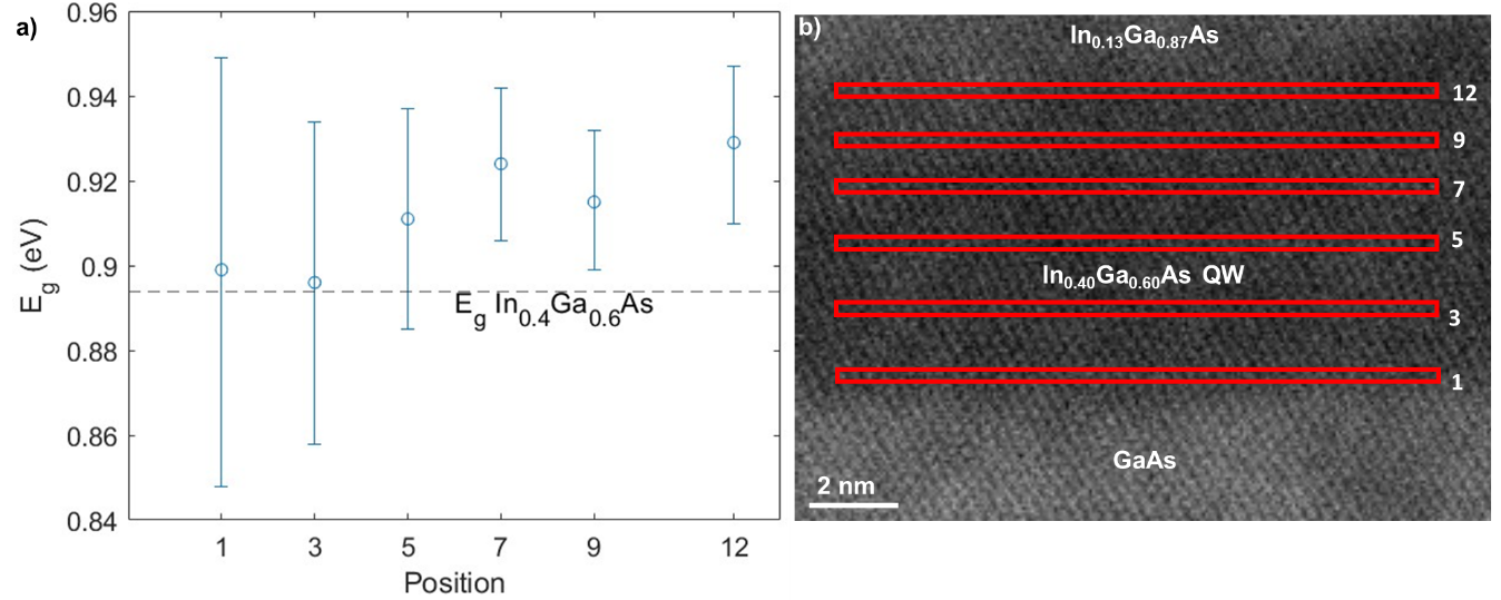
Figure 1 illustrates some of the initial results, where a trend can be clearly seen. This is that the bandgap varies slightly across the In0.40Ga0.60As QW, increasing from the bottom interface GaAs layer (a control interface layer, known as CIL) to the In0.13Ga0.87As barrier interface. The values compare well to those assuming a uniform concentration, where Eg = 0.893eV 5. Importantly, our work considers several factors that might influence the measured Eg including the background model, the fitting range used on the parabolic curve and smoothing6.
Figure 1a-b: Eg measurement in the InGaAs QW (a) as a position outlined in the STEM image (b). Data provided from measurements with 0.20eV-0.60eV background window, 0.95-1.15eV fitting range on parabola and no filter.
The strain maps for the corresponding area containing the QW indicate the higher relative strain in the growth direction (εyy) at the interface between the QW and the GaAs CIL. Importantly, the variation on the strain values across the QW area correlate with the variation in the Eg.
In conclusion, our study investigates changes in the band gap as a function of changes in the strain and chemical composition. Thus, providing a clearer understanding of the physical phenomena underlying the laser’s performance and which should be considered in future laser designs.
- References
1. Mura, E. E. et. al. Importance of Overcoming MOVPE Surface Evolution Instabilities for >1.3 μm Metamorphic Lasers on GaAs. Cryst. Growth Des. 21, 2068–2075 (2021).
2. Rafferty, B. & Brown, L. M. Direct and indirect transitions in the region of the band gap using electron-energy-loss spectroscopy. Phys. Rev. B 58, 10326–10337 (1998).
3. Fung, K. L. Y. et al. Accurate EELS background subtraction – an adaptable method in MATLAB. Ultramicroscopy 217, 113052 (2020).
4. Hÿtch, M. J., Snoeck, E. & Kilaas, R. Quantitative measurement of displacement and strain fields from HREM micrographs. Ultramicroscopy 74, 131–146 (1998).
5. Nahory, R. E., Pollack, M. A., Johnston, W. D. & Barns, R. L. Band gap versus composition and demonstration of Vegard’s law for In1-xGaxAsyP1-y lattice matched to InP. Appl. Phys. Lett. 33, 659–661 (1978).
6. Keller, D. et al. Local Band Gap Measurements by VEELS of Thin Film Solar Cells. Microsc. Microanal. 20, 1246–1253 (2014).