High resolution structural characterisation of silicon-vacancy colour centres in diamond using 4D-STEM and ptychography
- Abstract number
- 88
- Presentation Form
- Poster
- DOI
- 10.22443/rms.mmc2023.88
- Corresponding Email
- [email protected]
- Session
- Poster Session Two
- Authors
- Mr Aidan Horne (1), Mr Xiaopeng Wu (1), Dr Ben Green (1), Dr Peng Wang (1)
- Affiliations
-
1. Department of Physics, University of Warwick
- Keywords
4D STEM, Ptychography, Electron microscopy, Diamond, Colour centre, Photonics, Quantum computation
- Abstract text
In this work, we use a combination of atomically-resolved scanning transmission electron microscopy (STEM), 4D STEM and electron energy-loss spectroscopy (EELS) to uncover the structural details of Si-Vacancies (SiV) Centre in diamond, such as atomic configuration and bonding arrangement.
SiV centres in diamond are an area of research that has gained a lot of interest in recent years. SiV centres in diamond have been demonstrated as an effective coherent single photon emitter [1] which opens the door to potential uses in quantum communications and computing [2-6]. The structure of the defects plays an important role in defining optical properties. To enable the engineering of these defects in diamond so that they are created with the desired atomic structures: orientation, location and environment, it is essential to directly visualise their atomic structure and local chemistry at a high spatial resolution.
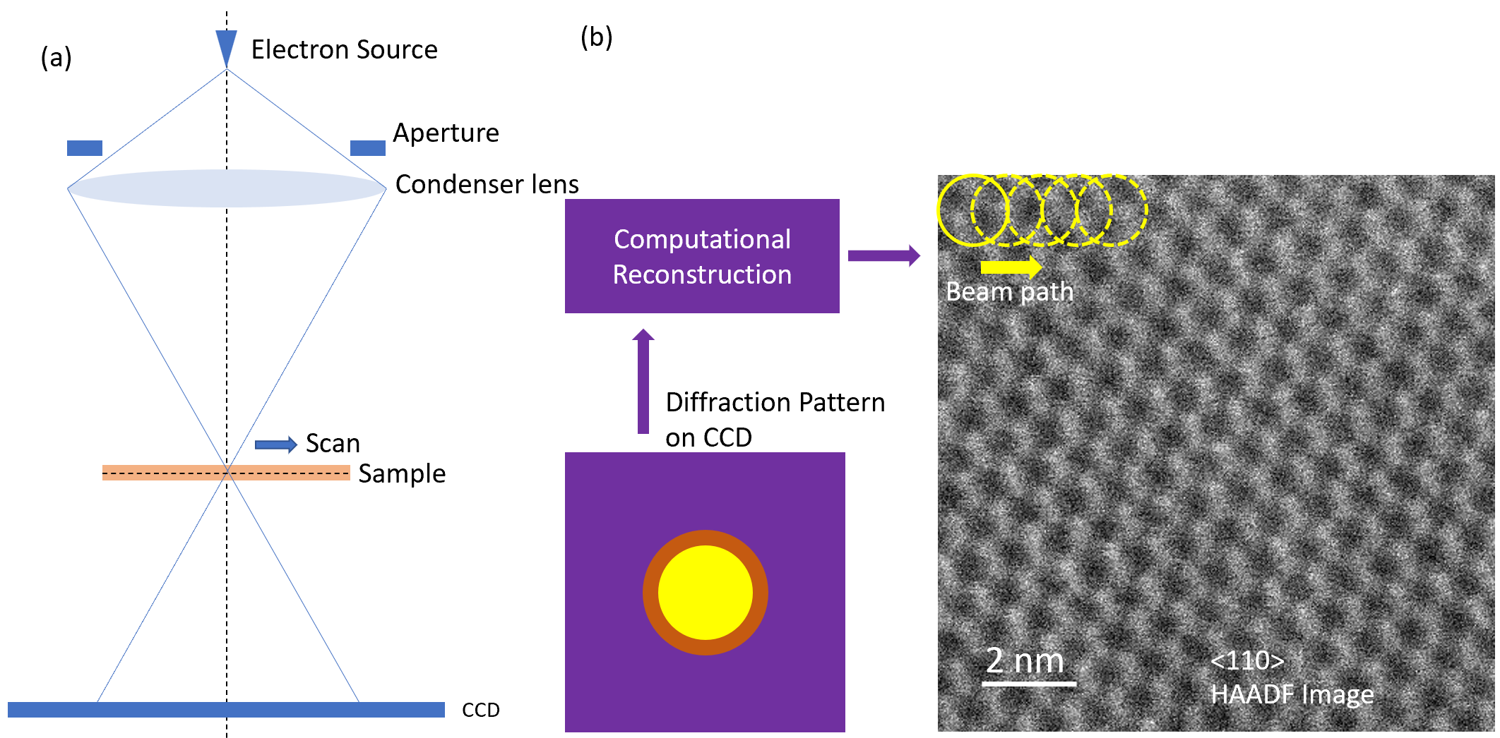
Recently, ptychography has attracted a tremendous attention as this approach has shown great potential in applications such as super-resolution imaging [7, 8], high-contrast light-element detection [9], low dose imaging [10], three-dimensional imaging [11, 12] and cryogenic bioimaging [13]. Figure 1 shows that a ptychographic 4D dataset can be acquired by scanning a focused or defocused probe over a specimen with highly overlapping probe positions. Ptychography can provide phase images of a sample with super resolution [14] and high contrast [9], which can potentially allow the locations of single atom defects to be directly visualised with high precision. The phase will be subequently correlated with structural models using image simulations. This study will shed light on how the SiV defect is formed and fabricated and discover structures of different types of defect.
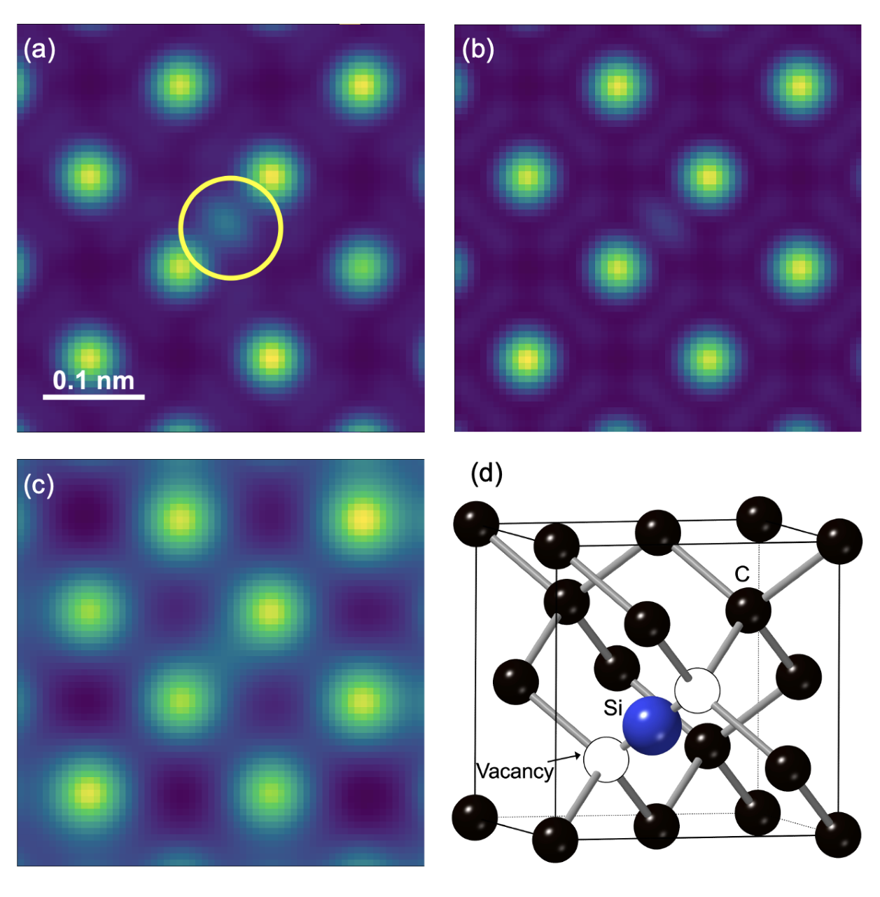
The SiV colour centre diamond sample was prepared by implanting silicon into the diamond followed by high temperature annealing [15]. The implantation energy was 500keV and the dose was 8x1013cm-2. This creates SiV centres 200nm below the surface of the diamond. These centres adopt a "semi-vacancy" position where the silicon replaces two carbon atom sites and sits between the two as shown in Figure [number]. The TEM sample was prepared using a TESCAN Amber FIB-SEM. The atomic resolved HAADF image (Figure 1) taken on an aberration corrected JEOL ARM200F STEM, shows the bright contrast of single silicon atoms sitting between C-C dumbbell in the diamond crystal lattice. The HAADF, iCOM and dCOM images (Figure 2 (a-c)) were simulated using abTEM [16] based on the atomic model of SiV centre in the diamond structure (Figure. d), which clearly show the location of a SiV centre indicated with a red circle. It can be anticipated that the direct imaging of the SiV centres in the diamond will bring new opportunities for facilitating defect engineering, eventually tailoring optical and electronic properties of SiV centre diamond.
Figure 1: (a) Diagram of the optical setup used for the collection of data for the ptychographic reconstruction. (b) The ptychographic reconstruction process from 4D-STEM data.
Figure 2: (a-c) Show simulations of 4D-STEM images along the <001> zone axis. (a) HAADF image, the Si atom is in the yellow circle. (b) dCoM image. (c) iCoM image. (d) Ball-Stick model of SiV colour centre in diamond lattice.
- References
[1] L. Marseglia et al., Opt. Express 26, (2018), p. 80–89.
[2] J. R. Weber et al., Journal of Applied Physics 109, 102417, (2011).
[3] S. Weng et al., Applied Physics Letters 119, 171101, (2021).
[4] D. Gavinsky et al., Association for Computing Machinery, (2007), p. 516–525
[5] PD. Nellist et al., Nature 374 (1995), p. 630.
[6] Y. Jiang et al., Nature 559 (2018), p. 343.
[7] A. Sipahihil et al., Science 354 (2016), p. 847-850.
[8] P. J. Stas et al., Science 378 (2022), p. 557-560.
[9] P. Wang et al., Scientific Reports 7 (2017), p. 2857.
[10] J. Song et al., Scientific Reports 9 (2019), p. 3919.
[11] S. Gao et al., Nature Communications 8 (2017), p. 163.
[12] Z. Ding et al., Nature Communications 13, (2022), p. 4787.
[13] L. Zhou et al., Nature Communications 11, (2020), p. 2773.
[14] Y. Jiang et al., Nature 559, (2018), p. 343–349.
[15] T. Schröder et al., Nature Communications 8, (2017), p. 2773.
[16] J. Madsen & T. Susi, Open Research Europe 1, (2021), p. 24.