Developments in designing a retrofittable photoelectron source for low voltage electron microscopy
- Abstract number
- 236
- Presentation Form
- Poster & Flash Talk
- DOI
- 10.22443/rms.mmc2023.236
- Corresponding Email
- [email protected]
- Session
- EMAG - 3D & Tomographic Electron Microscopy
- Authors
- Frances Quigley (2, 1), Clive Downing (1), Dr Cormac McGuinness (2), Dr Lewys Jones (2, 1)
- Affiliations
-
1. Advanced Microscopy Laboratory, Centre for Research on Adaptive Nanostructures and Nanodevices (CRANN)
2. School of Physics, Trinity College Dublin
- Keywords
Low voltage imaging, Scanning Electron Microscopy, Photoelectric effect, Photoelectron emitter, Electron gun
- Abstract text
Low voltage scanning electron microscopy (<5 keV) has become increasingly valuable in various research fields. The semiconductor industry benefits from the reduction in knock on damage [1], while its ability to produce detailed images of surface features can be extremely valuable in the area of material science [2]. The imaging however is hindered by the increased effect of chromatic aberration on resolution at lower voltages. Decreasing the energy spread of the electron beam is one solution to reducing the effect of the chromatic defocus blur. This is usually achieved by purchasing a SEM with a lower energy spread electron gun such as a Schottky field emitter (∆E≈0.7eV).
This work presents a novel design for a low energy spread electron emitter for a scanning electron microscope (SEM). Our solution utilizes the photoelectric effect where photons from a laser diode stimulate the direct release of electrons from the low workfunction material Lanthanum Hexaboride (LaB6). Previous research has shown that electron emitters of this nature can produce electrons with an energy spread as low as 0.11eV [3]. Using fibre optics and a UV laser diode, we have developed a prototype that can be retrofitted onto our existing thermionic LaB6 electron gun in a ZEISS EVO SEM.
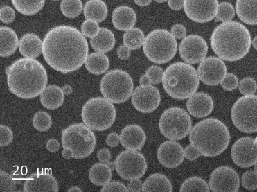
We will describe the initial design and latest version of this photoelectron emitter. This includes a higher-powered laser for increased photoelectron current as well as a new container for the light source for easier installation of the set up. Our results show that this photoelectron emitter delivers a continuous electron beam for SEM imaging (see Figure 1) and an analysis on how the laser power can control emitter current will be examined. COMSOL simulations have also been performed to determine the optimal bias to operate the emitter. An investigation into the properties of the photoelectron prototype in comparison to a thermionic gun will also be presented. This new design potentially offers an upgrade to existing thermionic SEMs, increasing their performance and usability for low voltage imaging research.
Figure 1: SEM image of Titanium balls imaged with the photoelectron emitter prototype. A 405nm 400mW UV laser was used and the LaB6 was at a temperature of 930K to minimize crystal contamination.
- References
[1] J.B. Pawley, Low Voltage Scanning Electron Microscopy, Scan. Electron Microsc. 3 (1984).
[2] J. Liu, High-resolution and low-voltage FE-SEM imaging and microanalysis in materials characterization, Mater. Charact. 44 (2000) 353–363. https://doi.org/10.1016/S1044-5803(99)00076-5.
[3] H. Sawa, M. Anzai, T. Konishi, T. Tachibana, T. Hirayama, Development of a UHV-compatible Low-energy Electron Gun using the Photoelectric Effect, J. Vac. Soc. Japan. 60 (2017) 467–470. https://doi.org/10.3131/jvsj2.60.467.
[4] FQ is supported by a Trinity College Provost’s Award scholarship. LJ is supported by Science Foundation Ireland grant number URF/RI/191637.