Determination of electric fields in ferroelectric domains using 4D-STEM
- Abstract number
- 82
- Presentation Form
- Poster
- DOI
- 10.22443/rms.mmc2023.82
- Corresponding Email
- [email protected]
- Session
- Poster Session Two
- Authors
- Yining Xie (1), Eoin Moynihan (1), Luca Reina (1), Prof. Marin Alexe (1), Prof. Richard Beanland (1), Prof. Ana M. Sanchez (1)
- Affiliations
-
1. University of Warwick
- Keywords
4D-STEM, electric fields, ferroelectrics, domains
- Abstract text
Advanced nanoscale characterization methods including piezoresponse force microscope (PFM) and transmission electron microscope (TEM), have been applied to many different domain structures (such as domain walls, vortices, and Skyrmions) in low dimension ferroelectric materials (Meier & Selbach, 2021). Although, accurately determining electric fields, and thus polarization, around domain walls at atomic resolution is still challenging.
Scanning transmission electron microscope (STEM) provides a variety of functions in atomic scale combining different detectors and analysis methods. By using high performance pixeled electron detector, a 2D diffraction pattern may be recorded at each position of the 2D scanning area, so called four-dimensional STEM (4D-STEM) (Ophus, 2019). Plenty of information may then be extracted from the 4D dataset with computational methods.
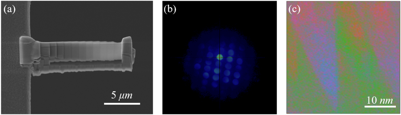
This work uses a combination of a double aberration-corrected JEOL ARM and a Quantum Detectors Merlin pixelated direct electron detector to realize 4D-STEM. The electric fields across domain wall interfaces are measured in different perovskite ferroelectrics, such as single crystal BiFeO3 (BFO) and PbTiO3 (PTO), with a range of sample thicknesses. Thickness stepping samples are made using focused ion beam (FIB) to get a parallel sided area for each step in the lamella, as shown in Fig1.(a). LiberTEM and other Python packages are then used to process the 4D dataset (Clausen et al., 2022). Fig1.(b~c) illustrate a centre of mass (CoM) shift across a 180 degree ferroelectric domain wall in a BFO single crystal along the [1-10] zone-axis to represent the field change across the scanning area, by applying a disk mask on the diffraction pattern. This work establishes the influence of specimen thickness on electric field measurements in ferroelectric domain structures using 4D-STEM.
Figure1: (a) SEM image of a stepped PTO sample on a grid (10 keV); (b~c) 4D dataset of a BFO single crystal sample along [1-10] direction, in which (b) 2D diffraction pattern recorded on the detector (c) centre of mass calculation on the scanning area.
- References
Clausen, A., Weber, D., Bryan, M., Ruzaeva, K., Migunov, V., Baburajan, A., Bahuleyan, A., Caron, J., Chandra, R., Dey, S., Halder, S., Katz, D. S., Levin, B. D. A., Nord, M., Ophus, C., Peter, S., Puskás, L., Schyndel van, J., Shin, J., . . . Dunin-Borkowski, R. E. (2022). LiberTEM/LiberTEM: 0.10.0. In [Software]. https://doi.org/10.5281/zenodo.6927963
Meier, D., & Selbach, S. M. (2021). Ferroelectric domain walls for nanotechnology. Nature Reviews Materials, 7(3), 157-173. https://doi.org/10.1038/s41578-021-00375-z
Ophus, C. (2019). Four-Dimensional Scanning Transmission Electron Microscopy (4D-STEM): From Scanning Nanodiffraction to Ptychography and Beyond. Microsc Microanal, 25(3), 563-582. https://doi.org/10.1017/S1431927619000497