The field-emission regime of STM for spintronic and 2D materials
- Abstract number
- 355
- Presentation Form
- Poster
- DOI
- 10.22443/rms.mmc2023.355
- Corresponding Email
- [email protected]
- Session
- Poster Session Two
- Authors
- Dr. Gabriele Bertolini (1), Oskar Fossberg (1), Dr. Andrew Pratt (1), Prof. Steve Tear (1)
- Affiliations
-
1. School of Physics, Engineering and Technology, University of York
- Keywords
Field emission, 2D materials, Spintronics, Scanning Probe Microscopy.
- Abstract text
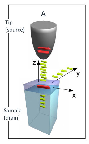
The field-emission regime [1] of a Scanning Tunneling Microscope (STM) occurs when the tip-sample distance is more than few nanometres (~ 5-100 nm), and tip bias voltage is enough to field-emit electrons at the tip (~ - (10-100) V). In this configuration the direct electron tunneling between the ultimate atoms on the tip apex and the sample surface underneath is forbidden, but a sharp tip becomes a source of electrons due to field emission (fig. 1A). The emitted electrons hit the target and cause the generation of secondary electrons (elastic and inelastically scattered) on the sample surface. Such excited electrons can escape from the tip-sample junction and may be collected by several means and analysed, allowing both microscopy and spectroscopy investigations [2, 3].
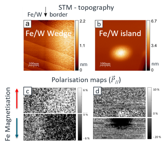
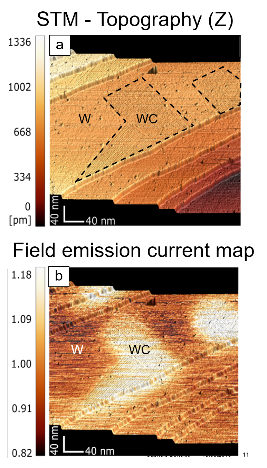
The strong dependence of the physical properties of the secondary electrons on the nature of the sample surface, due to their low energy (<100 eV), makes complementary information accessible. Besides the absorbed current maps and the z-piezo displacement images of the surface (as in STM), chemical and magnetic contrast with nanometre scale resolution can be achieved on the same region [4, 5, 6]. In this talk we give a short overview of the potential application of this spectroscopy/microscopy instrument to investigating both magnetic and electronic properties of nanostructures, thin film and 2D materials. For example in a study of Fe/W(110) (fig. 1B), the detection of spin polarised secondary electrons generated at the sample, has been used for magnetic imaging of the different magnetic domains [5]. In another study, Carbide(WC) domains on W(110), originate non-topographic field emission current contrast via the local variation of the work function at the surface (fig. 1C) [6].
(A) Tip-sample junction
(B) STM vs Spin polarisation
(C) STM vs Field emission
Fig. 1 – A) Tip acts as source of unpolarised primary electron beam. The electrons escaping the junction, in virtue of the spin-dependent electron scattering experienced at the surface, can have a non-zero spin polarisation depending on the surface magnetisation. Red arrows represent the magnetization of the tip and sample, while green arrows the spin states of propagated electrons. B) STM topography maps (a, b) of two different magnetic nanostructures of Fe/W and their corresponding magnetisation information residing on the secondary electron polarisation maps(c, d) [3]. C) STM topography(a) and field emission current map(b) of a WC domain embedded in W(110) terrace.
Acknowledgement(s): This project is supported by EPSRC grant EP/V012126/1 (SEE MORE MAKE MORE).
- References
[1] R. Young et.al. Rev. of Sci. Inst. 43, 999 (1972)
[2] R.E. Palmer et al. Surf. Sci., 502–503, pp. 224-231 (2002)
[3] R. Allenspach et. al. App. Phys. Lett. 54, 587 (1989)
[4] D. A. Zanin et al Pro. Roy. Soc. A 472, 20160475 (2016)
[5] L. De Pietro et al., Sci. Rep. vol. 7, 13237 (2017)
[6] G. Bertolini et al. R. Soc. Open Sci. 2021, 8, 5009064 (2021).