Simultaneous co-located Raman and SEM imaging for correlated SEM microscopy
- Abstract number
- 14
- Presentation Form
- Poster & Flash Talk
- DOI
- 10.22443/rms.mmc2023.14
- Corresponding Email
- [email protected]
- Session
- Multiscale and Correlative Microscopy Approaches to Microanalysis and Spectroscopy
- Authors
- Jorge Diniz (1), Pete Johnson (1), Tim Smith (1)
- Affiliations
-
1. Renishaw plc
- Keywords
Raman spectroscopy, Raman imaging, SEM, correlative microscopy, 2D materials, Geology
- Abstract text
Scanning electron microscopy (SEM) is a powerful technique for structural and elemental analysis of a wide range of materials. In contrast, Raman spectroscopy is a complimentary optical technique that provides information on the chemical bonding and structure. When combined, SEM analysis can be used to locate structures or defects at high spatial resolution, while Raman spectroscopy can be used to determine chemical information with high specificity. Correlating the information from these techniques leads to a greater understanding of the specimen. It is important however, that the data and images from the different modalities can be directly and accurately aligned without positional errors that could be caused when moving samples to different analysis positions or equipment. In this work, we demonstrate the inLux SEM Raman interface which, when attached to a SEM chamber, is capable of simultaneous and co-incident SEM and Raman imaging from the same sample position, thus avoiding correlation errors.
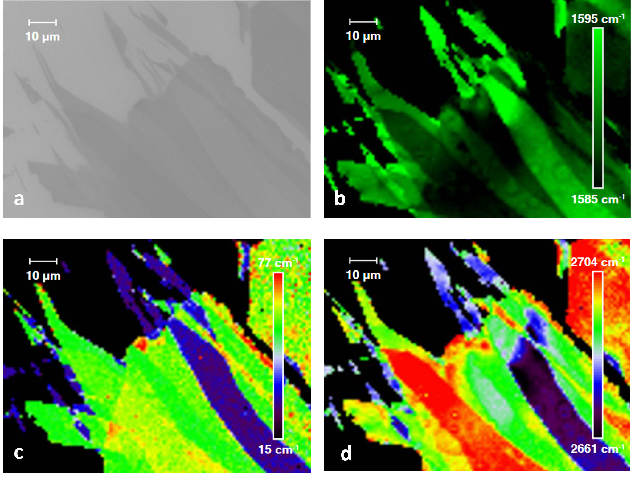
Figure 1 shows SEM and Raman images acquired from single and multi-layer graphene. Over 11,000 spectra were collected by moving the inLux probe, while the sample remains stationary inside the SEM. In contrast to the SEM image, the information-rich Raman images of the carbon G band and 2D bands visualise layer thicknesses and strain.
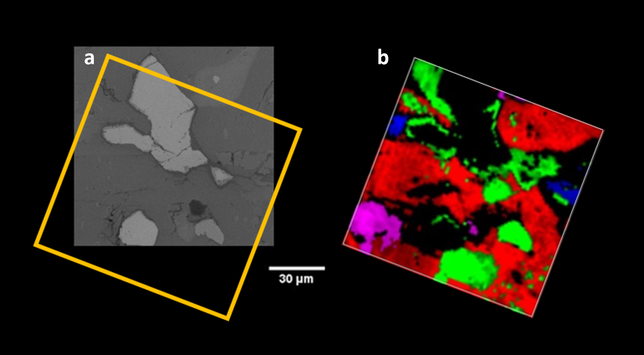
Figure 2 illustrates SEM and Raman images taken from a mineral section. This demonstrates clear and accurate overlay between SEM and Raman features. Additionally, Raman imaging detected additional information with the presence of biotite which is not visible in the SEM image.
We demonstrate with these examples how Raman and SEM can increase understanding of materials, the complementary nature of the techniques, and their power when combined.
Figure 1: (a) SEM secondary electron image of graphene corresponding to the same area as the Raman images shown. (b) Raman image of G band position, an indicator of local strain and doping in the graphene layers. (c) Raman image of the graphene 2D band width, an indicator of the number of graphene layers. Single layer material (blue), few layer material (green), and thicker material in (yellow/red). (d) Raman image of 2D band position; this can be used to understand the local electronic properties of the graphene.
Figure 2: (a) SEM image of mineral section (b) Corresponding Raman image illustrating the distribution of rutile (green), oligoclase (red), biotite (blue) and amphibole (purple).