A study on the anomalous effects of strain in selected area diffraction patterns (SADP) due to boron doping in silicon
- Abstract number
- 158
- Presentation Form
- Contributed Talk
- DOI
- 10.22443/rms.mmc2023.158
- Corresponding Email
- [email protected]
- Session
- EMAG - Microscopy of Semiconductors
- Authors
- Miss Kaviyadharshini Dhamotharan (1), Dr Budhika Mendis (1)
- Affiliations
-
1. Durham University
- Abstract text
Semiconductors have a significant impact on our lives due to their role in the fabrication of electrical devices. The sensitivity of its conductivity to temperature, illumination, magnetic field, and minute amount of impurity atoms make semiconductors one of the most important materials for electronic applications. It is important to study defects since it alters the electrical properties of a semiconductor in a massive way. Microscopic lattice defects such as point defects, dislocations induce local electronic density of state changes and distort the lattice structure surrounding the defects. The effect these interruptions of the crystal lattice have on the scattering of photons or charged particles such as electrons can be used to study the defect.
The effect of static atomic displacements associated with misfitting boron atoms in silicon (B-Si) has been studied using high angle annular dark-field (HAADF) imaging by Perovic et al (1). It was found that the HAADF contrast of the boron doped silicon (B-Si) layer is brighter than elemental silicon (Si), despite the decrease in atomic number. This could be due to static atomic displacements arising solely from the displacement of Si atoms from their equilibrium lattice sites adjacent to substitutional boron atoms (2). This type of contrast is called Huang scattering contrast. In addition, high concentrations of boron can also modify the phonon properties of the material (3), which affects the thermal diffuse scattering (TDS). Perovic et al. (1) had attributed the anomalous HAADF contrast to TDS, although the effects of Huang scattering were not considered.
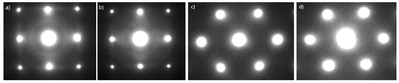
We have used transmission electron microscopy (TEM) to analyse strain around point defects in silicon highly doped with boron, i.e., degenerate doping (B-Si). Fig 1 shows selected area diffraction patterns (SADPs) of elemental Si and B-Si from [100] and [110] zone-axis orientations. For [100] Si (Fig 1a) there is streaking arising from acoustic phonon scattering along [010] and [001] crystallographic directions around the Bragg reflections. The halo ring pattern around the unscattered beam is thought to be due to surface contamination. For [100] B-Si (Fig 1b), the streaking is reduced, which could be due to the smaller thickness of this sample. However, diffuse scattering in the form of a cross-shaped pattern between the unscattered and 020 Bragg beams is evident. The diffuse scattering is not observed for elemental Si, suggesting modification of phonons due to boron doping. This is also consistent with our Raman results, which shows significant peak broadening upon degenerate doping. It should be noted that anomalous low angle scattering due to boron was not observed in other zone-axis orientations, such as [110] (Figs. 1c and 1d).
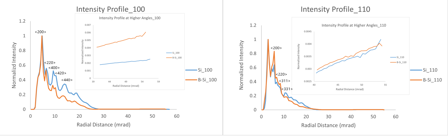
Radial intensity profiles from Si and B-Si are obtained from the [100] and [110] zone-axis diffraction patterns (Fig 2). The total intensity has been normalised for a direct comparison. For [100] the (t/lambda) specimen thickness ratio, measured using electron energy loss spectroscopy, was 0.75 for B-Si and 1.01 for Si. Therefore, at high scattering angles the intensity for Si should be higher than B-Si due to the larger atomic number (Z) and specimen thickness. However, the opposite trend is observed (Fig 2a), which is also consistent with the previous results of Perovic et al. [1]. The anomalous high angle scattering is also observed for [110], although its effects is smaller (Fig 2b; the (t/lambda) ratio for the two samples were similar, i.e., 0.71 for B-Si and 0.67 for Si).
The diffraction intensity at high scattering angles is due to localised scattering, and therefore we expect the intensity to be dominated by Huang scattering from the boron point defect atoms. On the other hand, the diffuse scattering in the zero order Laue zone pattern is likely to be dominated by phonons, and here we find evidence of changes in the phonon configuration due to boron doping.
Fig 1: Diffraction patterns (DP) of Si and B-Si for different zone axes. a) Si DP for [100]; b) B-Si DP for [100]; c) Si DP for [110]; d) B-Si DP for [110].
Fig 2: Comparison of radial intensity profiles (IP) of Si and B-Si for different zone axes. a) IP comparison for zone axis [100]; b) IP comparison for zone axis [110].
In summary, the effect of strain due to point defects has been studied in boron doped silicon using SADPs from [100] and [110] zone axes. Anomalous diffuse scattered intensity is observed at both small and large scattering angles. It is concluded that boron gives rise to Huang scattering due to the intrinsic strain in the lattice, as well as altering the phonon configuration, and hence thermal diffuse scattering. Future work will look to acquire diffraction data under liquid nitrogen cooling, which suppresses the TDS, but not Huang scattering.
- References
1) D.D. Perovic, C.J. Rossouw, and A. Howie, Imaging elastic strains in high-angle annular dark field scanning transmission electron microscopy. Ultramicroscopy, 52(3):353–359, 1993.
2) Peisl, H. "Defect properties from x-ray scattering experiments." Le Journal de Physique Colloques 37.C7 (1976): C7-47.
3) Bourgeois, E., and X. Blase. "Superconductivity in doped cubic silicon: An ab initio study." Applied physics letters 90.14 (2007): 142511.