Correlative atomic resolution electron imaging of grain boundaries and intragrain between interfaces in perovskite semiconductors
- Abstract number
- 476
- Presentation Form
- Poster
- DOI
- 10.22443/rms.mmc2023.476
- Corresponding Email
- [email protected]
- Session
- Poster Session Three
- Authors
- Miss Xinjuan Li (1)
- Affiliations
-
1. Department of Material Science ad Metallurgy, University of Cambridge
- Keywords
HRSTEM, atomic resolution, Hybrid perovskite thin films, electrically active intragrain, defects
- Abstract text
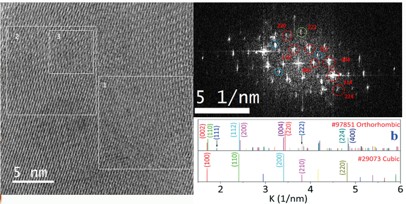
The location and distribution of dopants, impurities, and defects within the perovskite layer and at the interfaces with other layers in perovskite solar cells can have a significant impact on the performance and stability of the device. Therefore, it is important to understand the nature and distribution of these materials in the device. Atomic resolution microscopy can be used to visualize and characterize these defects, study the location and distribution of dopants, and identify and locate these impurities at the atomic scale, providing insights into their effect on the transport and recombination of charge carriers within the device and the structure and electrical properties of the perovskite layer. Here, we propose a correlative study between the structural and electrical properties of such dopants, impurities, and defects at atomic resolution. Perovskite solar cell device samples with various defect properties and densities will be correlatively studied using PEEM, CL, EBSD and HRSTEM to understand structural and compositional characteristics. From interpreting the lamella structure of the perovskite layer, as the image is taken along[1-10] zone axis, (110),(112),(114),(002),(114) and (224) spots are identified. The other reciprocal lattice vectors, with lengths of 3.39 nm−1 measured from weak (222) spots (marked with green circles), which were unique for the orthorhombic (ICSD 97851) phase and were missing in the cubic (ICSD 29073) and tetragonal (ICSD 109295) phases, used as evidence to indicate the phase transition from cubic to orthorhombic phases after cooling down to room temperature. A few diffraction spots, marked in Blue circles are missed identification. Possible assumptions may give that they are the precipitate from CsPb and Pb after the degradation and decomposition of perovskite thin films. The formation of secondary phases of Cs4PbBr6 or Cs2PbBr5 due to excess Cs are the other possibilities, which will be further confirmed with STEM-EDX, PL/CL studies.
Fig.1. Typical HRSTEM and FFT images of the CsPbBr3 perovskite thin films, with standard patterns for the orthorhombic (ICSD 97851) and cubic (ICSD 29073) phases.[Ref: CrystEngComm, 2017, 19, 679 ]
- References