Measuring Electric Fields using 4D-STEM: Experimental Optimisation, Simulation, and Post-Processing
- Abstract number
- 195
- Presentation Form
- Contributed Talk
- DOI
- 10.22443/rms.mmc2023.195
- Corresponding Email
- [email protected]
- Session
- EMAG - 4D STEM
- Authors
- Eoin Moynihan (2), Yining Xie (2), Luca Reina (2), Prof. Marin Alexe (2), David Cooper (1), Prof Richard Beanland (2), Prof. Ana M. Sanchez (2)
- Affiliations
-
1. Univ. Grenoble Alpes, CEA-LETI
2. University of Warwick
- Keywords
4D-STEM, electric field mapping, p-n junction, ferroelectric, electron microscopy
- Abstract text
Fast pixelated detectors have revolutionized the acquisition of data inside the transmission electron microscope (TEM). [1] We are now able to acquire electron diffraction data localized down to the atomic scale using scanning TEM (STEM). With this leap forward in capability it means new opportunities are available to us, but it also means new challenges. For each position of the convergent STEM probe on our sample, we can record a convergent beam electron diffraction (CBED) pattern. This experiment results in a four-dimensional (4D) dataset giving us the umbrella term 4D-STEM for a powerful technique. [2] Our research uses 4D-STEM to measure the electric field in material interfaces such as ferroelectric domain walls and semiconducting p-n junctions.
This work uses the JEOL-ARM double-aberration corrected STEM equipped with a field emission gun and electron energy loss spectrometer (EELS). 4D-STEM is made possible using the Merlin direct electron detector from Quantum Detectors, based on Medipix3 technology. [3] Post-processing used the LiberTEM python package. [4] Multislice simulations used a combination of AbTEM [5] and clTEM [6]
4D-STEM is a challenging technique to implement with large datasets, complex experimental designs, and strict sample requirements. Small long-range electric fields such as those across a p-n junction require an optimization of experimental parameters e.g. the convergence semi-angle, sample orientation and thickness, beam precession, or energy filtering. [7], [8] In our work we use a combination of experimental data, simulations, and data post-processing to create an open workflow for reproducible measurement of the electric field through 4D-STEM.
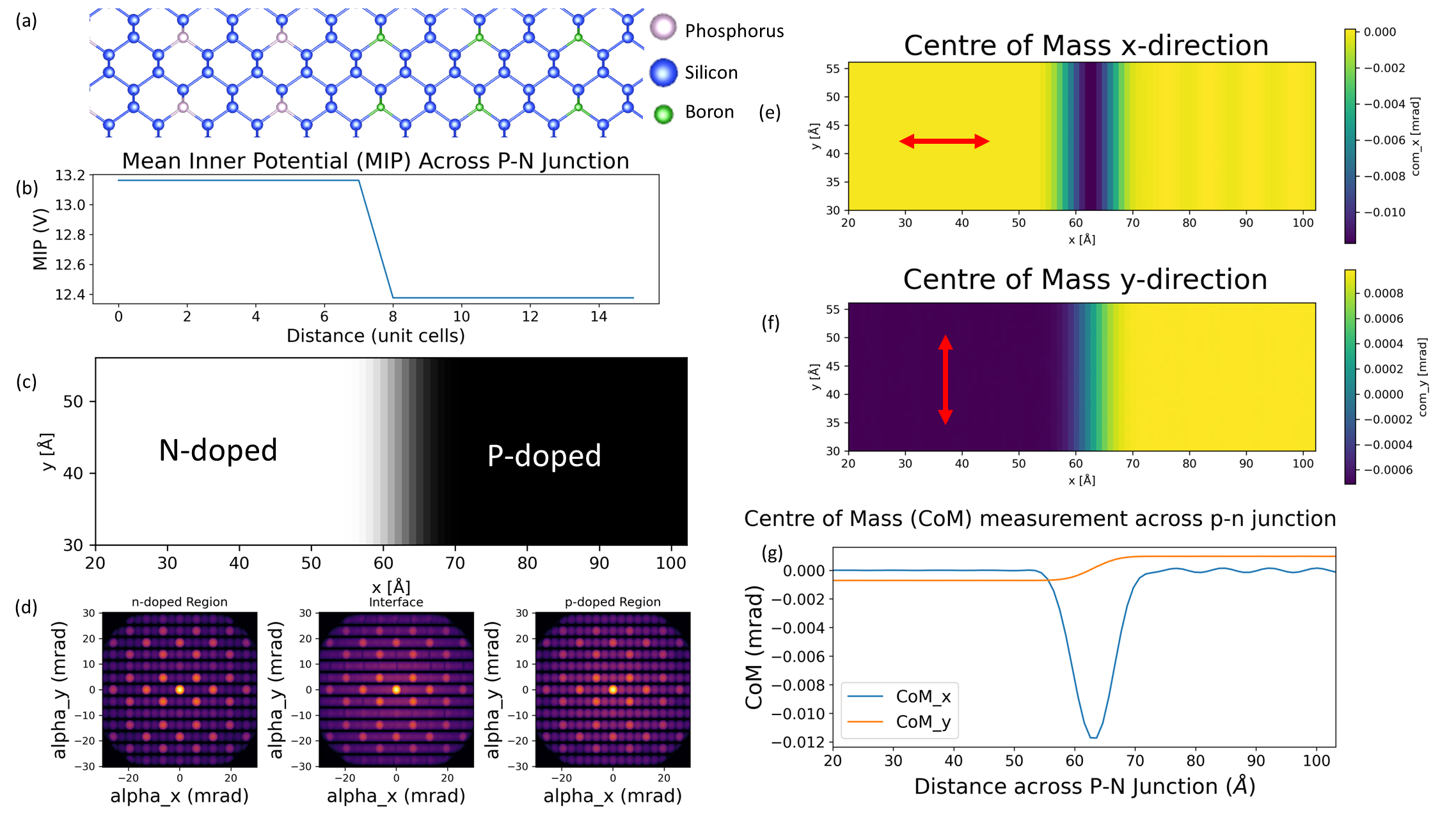
In Figure 1 we show an example of a multislice simulation of a 4D-STEM dataset using the Centre of Mass (CoM) to measure the deflection of the electron beam. The doping concentrations are quite high at about , but these simulations still show how the interactions between the electron beam and the sample can be measured through 4D-STEM measurements. In Figure 1 (g) we can see how the CoM measurement in the x direction (CoM_x) corresponds to a small deflection in the CBED pattern of about 10 μrad. The CoM_y measurement shows the influence of the atomic dipoles in the differently doped areas of the sample when projecting along the [110] direction. For doped silicon the effect is quite small, but for a semiconductor like AlAs this deflection caused by atomic dipoles can be larger than the deflection caused by the electric field at the p-n junction interface.
Simulations work in tandem with our experiments to help us understand the origins of our measurements. Through many iterations of different microscope parameters and sample conditions we can validate our experimental results, as well as choose the optimal setup for acquisitions. This project attempts to make a reliable workflow and methodology to standardise 4D-STEM as a tool for the measurement of electric fields.
Figure 1: Multislice simulations showing the deflection of the electron beam as it travels across a p-n junction for an electron beam of 200kV with a convergence semi-angle of 2 mrad. (a) atomic model of [110] silicon doped with phosphorus (n-dopant) and boron (p-dopant) (b) Mean Inner Potential calculated on both sides of the junction with similar methods to [8] (c) ADF image with low convergence semi-angle (d) CBED patterns across p-n junction (e) Centre of Mass measured in x-direction (f) Centre of Mass measured in y-direction, arrows show direction of deflection for CBED pattern (g) Profile across p-n junction showing the CoM.
- References
[1] B. D. A. Levin, “Direct detectors and their applications in electron microscopy for materials science,” Journal of Physics: Materials, vol. 4, no. 4, p. 042005, Jul. 2021, doi: 10.1088/2515-7639/AC0FF9.
[2] C. Ophus, “Four-Dimensional Scanning Transmission Electron Microscopy (4D-STEM): From Scanning Nanodiffraction to Ptychography and Beyond,” Microscopy and Microanalysis, vol. 25, no. 3, pp. 563–582, 2019, doi: 10.1017/S1431927619000497.
[3] R. Ballabriga, M. Campbell, E. Heijne, X. Llopart, L. Tlustos, and W. Wong, “Medipix3: A 64 k pixel detector readout chip working in single photon counting mode with improved spectrometric performance,” Nucl Instrum Methods Phys Res A, vol. 633, no. SUPPL. 1, pp. S15–S18, May 2011, doi: 10.1016/J.NIMA.2010.06.108.
[4] A. Clausen et al., “LiberTEM/LiberTEM: 0.10.0,” Jul. 2022, doi: 10.5281/ZENODO.6927963.
[5] J. Madsen, T. J. Pennycook, and T. Susi, “ab initio description of bonding for transmission electron microscopy,” Ultramicroscopy, vol. 231, Dec. 2021, doi: 10.1016/j.ultramic.2021.113253.
[6] J. J. P. Peters, “A Fast Frozen Phonon Algorithm Using Mixed Static Potentials,” Ultramicroscopy, vol. 229, p. 113364, Oct. 2021, doi: 10.1016/J.ULTRAMIC.2021.113364.
[7] B. C. da Silva et al., “The influence of illumination conditions in the measurement of built-in electric field at p–n junctions by 4D-STEM,” Appl Phys Lett, vol. 121, no. 12, p. 123503, Sep. 2022, doi: 10.1063/5.0104861.
[8] V. S. Chejarla, S. Ahmed, J. Belz, J. Scheunert, A. Beyer, and K. Volz, “Measuring spatially-resolved potential drops at semiconductor hetero-interfaces using 4D-STEM,” Jan. 2023, doi: 10.48550/arxiv.2301.11179.