A Novel Method for Minimising Contaminations for Sample Preparation Using FIB
- Abstract number
- 295
- Presentation Form
- Contributed Talk
- DOI
- 10.22443/rms.mmc2023.295
- Corresponding Email
- [email protected]
- Session
- FIB Applications & EM Samples Prep Techniques in Physical Sciences
- Authors
- Ms Xiangli Zhong (2), Mr Kerui Wei (2), Prof Ping Xiao (2), Prof Sarah Haigh (2), Prof Philip J Withers (1)
- Affiliations
-
1. Henry Royce Institute, School of Materials, University of Manchester
2. School of Materials, University of Manchester
- Keywords
focused ion beam (FIB), Cryo-FIB, insitu-transmission electron microscope (TEM), sample preparation
- Abstract text
The Focused Ion Beam (FIB) systems has become an important and popular tool for site-specific sample preparations for many characterization instruments including transmission electron microscopy (TEM), atomic probe (ATP), transmission Kikuchi diffraction (TKD) and microCT et al [1] [2]. Recently, many research groups on materials, physics, chemistry, and biological sciences has advanced into in-situ analysis at nanometre, molecular or atomic level in various environment to study matter’s thermal, chemical, mechanical and electrical properties[1]. The increasing popularity of MEMS based TEM chips has induced higher demand using FIB for the sample preparation[1]. Despite there are more and more FIBs applications, ion beam may induce damage or contamination issues especially to beam sensitive materials [3]. Contamination is a common issue on the FIB prepared samples which often hinder the accuracy of the analysis results[4]. The aim of this study is to propose and test a novel method to eliminate or minimise the contaminations on FIB prepared TEM samples.
An important aspect of conventional FIB or pFIB TEM specimen preparation involves the attachment of the FIB-produced lamella to an appropriate grid or chip support to facilitate subsequent TEM characterisation. During the attachment process, a CVD process is involved where a pad usually consists of a few micrometres thickness of Pt, W, C etc which depends on the CVD precursor applied. These CVD materials may pose potential interference with the pristine sample surface under testing environment no matter it is under temperature, chemical solutions/gases, electrical field, or mechanical force. To tackle this problem, we proposed, tested, and analysed a method making use of the intrinsic redeposition property of the ion beam processing during FIBing, knowingly as redeposition method. No ‘foreign’ CVD materials is involved, therefore, no contamination from ‘foreign’ material is introduced in this process hence eliminating contamination from it.
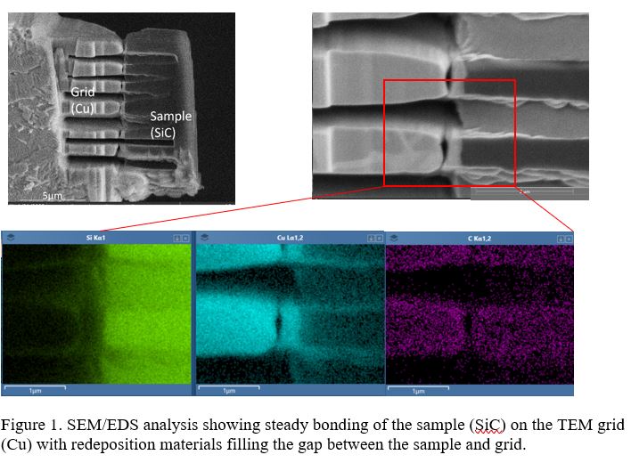
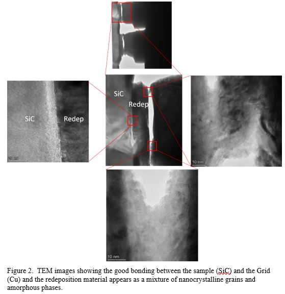
The redeposition materials is the result of ion – matter interactions where high energy ion beam bombards on the sample surface and sputters away the sample molecules/atoms. These sputtered materials are mostly pumped away by the high vacuum in the FIB chamber, however, there are some left in the close vicinity of the milling area which is defined as redeposition materials. These materials usually appear as nanoparticles with high surface area to volume ratio. They intend to minimise their surface area and stay together or stay at small openings to minimise their surface area. The combined effect of 1) attraction force between the nanoparticles, 2) the attraction force between the sample/grid/chip surfaces and the nanoparticles, enabled the bonding of these nanoparticles formed redeposition materials with the sample and grid surfaces. Figure 1 shows a SiC sample was attached to a Cu grid by redeposition materials. The SEM image and EDS analysis confirmed the redeposition materials filling at the gap between the sample and the grid. Figure 2 is the TEM image showing the good bonding between the sample (SiC) and the redeposition materials. The redeposition materials appears as a mixture of nanocrystalline gains and amorphous phases.
- References
[1] X. L. Zhong, S. Schilling, N. J. Zaluzec, and M. G. Burke, “Sample preparation methodologies for in situ liquid and gaseous cell analytical transmission electron microscopy of electropolished specimens,” Microsc. Microanal., vol. 22, no. 6, 2016, doi: 10.1017/S1431927616011855.
[2] S. M. Vitale and J. D. Sugar, “Using Xe Plasma FIB for High-Quality TEM Sample Preparation,” Microsc. Microanal., vol. 28, no. 3, pp. 646–658, 2022, doi: 10.1017/S1431927622000344.
[3] D. M. Long, M. K. Singh, K. A. Small, and J. Watt, “Cryo-FIB for TEM investigation of soft matter and beam sensitive energy materials,” Nanotechnology, vol. 33, no. 50, 2022, doi: 10.1088/1361-6528/ac92eb.
[4] X. Zhong et al., “Comparing Xe+pFIB and Ga+FIB for TEM sample preparation of Al alloys: Minimising FIB-induced artefacts,” J. Microsc., no. July, pp. 1–12, 2020, doi: 10.1111/jmi.12983.