Revealing the surface properties of InN nanoparticles via near-field microscopy
- Abstract number
- 174
- DOI
- 10.22443/rms.mmc2023.174
- Corresponding Email
- [email protected]
- Authors
- Xinyun Liu (2), Rajiv Prinja (1), Dr Baset Gholizadeh (2), Daniel Johnson (2), Dr Tom Vincent (2), Prof Nazir P. Kherani (1, 3), Dr Jessica L. Boland (2)
- Affiliations
-
1. Department of Electrical & Computer Engineering, University of Toronto
2. Photon Science Institute, University of Manchester
3. Department of Materials Science & Engineering, University of Toronto
- Keywords
Indium Nitride, s-SNOM, Scattering Scanning Near-field Optical Microscopy, FTIR, Oxidisation identification
- Abstract text
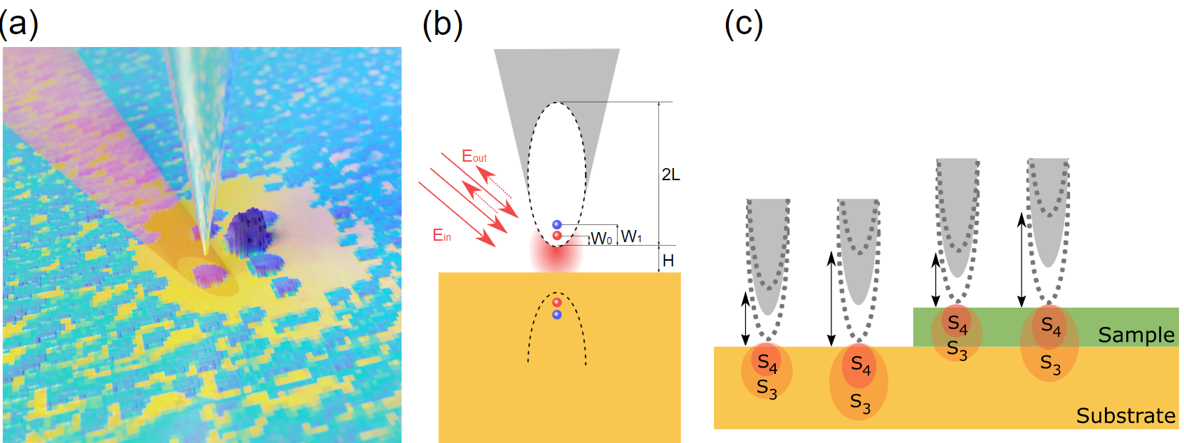
Scattering type scanning near field optical microscopy (s-SNOM) is a powerful technique for surface analysis, allowing imaging and spectroscopy on nanometre length scales [1]. s-SNOM utilises an AFM based instrument, where a light source is coupled to the apex of a sub-wavelength (nanoscale) AFM tip (Figure 1a-b). The light experiences strong field confinement, generating an evanescent (near-field) at the tip apex that interacts with the sample. Then the light scatters back in the far-field to detector carrying the near field sample information. In our experiments, s-SNOM is conducted in tapping-mode, with the tip oscillating at a set frequency. The near field signal is then modulated at harmonic orders of the tip-tapping frequency. As the background signal remains unmodulated, the near-field signal can be separated from large background noise, providing local sample information. Due to the near-field exponential decay nature, s-SNOM is a perfect tool for surface analysis, as the probing depth can be tune down to 10s of nanometres from the surface.
Figure 1. (a) A schematic diagram of s-SNOM tip sample configuration. (b) Near-field interaction between tip and sample. (c) Different probing depth as function of tapping amplitude and demodualation order.
Among III-V materials, indium nitride (InN) has a relatively low electron effective mass and high drift velocity, which suggests the high potential in applications like optoelectronic devices and catalysis [2, 3]. Aspects such as lattice structure, defects, oxidation level, are important to evaluate the quality of growth. Although s-SNOM is a surface sensitive technique, the subsurface probing can go up to ~ 100 nm underneath sample surface via altering experimental parameters. [4, 5] In this study, we use s-SNOM to analyse InN particles grown by gas phase synthesis onto a gold substrate. We modified tapping amplitude and demodulation order to achieve different probing depths within the sample (Figure 1c). This allows us to take both surface-sensitive and bulk-sensitive measurements.
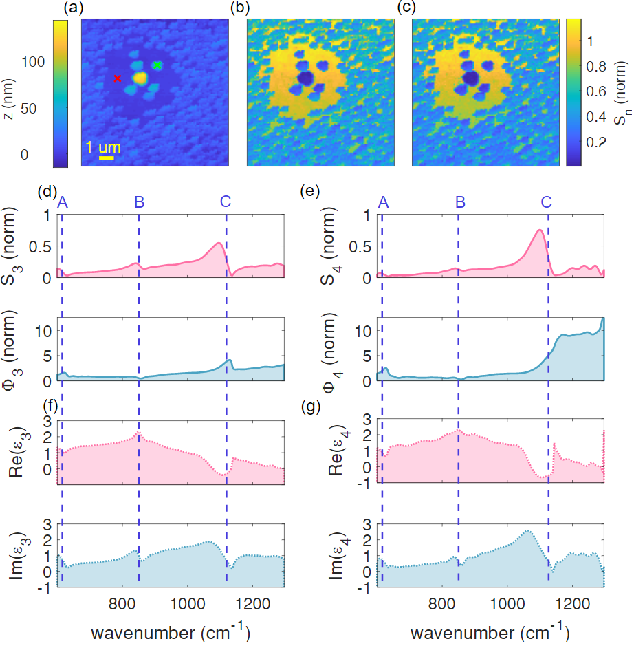
Figure 2. (a) AFM height, (b) 3rd demodulated amplitude and (c) 4th demodulated amplitude scan of area of interest. (d) 3rd and (e) 4th demodulated spectra taken from InN particle marked as green cross in (a), with normalization to gold substrate marked as red cross. (f) and (g) are dielectric function extracted from 3rd and 4th demodulated near-field signal via finite-dipole model.
As shown in figure 2a-c, during 2D scans, clear contrast between InN particles and gold substrate can be observed in all AFM height and optical signal 2D images. The optical contrast originates from the overall lower refractive index of InN compared to gold substrate. To identify the spectral feature, we performed spectroscopy on selected InN particles (marked as green cross in figure 2a). The InN spectra was normalized to gold reference (red cross in figure 2a) to eliminate any external systematic error. We noticed there are two clear resonances located at 850 cm-1 and 1150 cm-1, as well as a faint resonance at ~600 cm-1. We named these resonances, A (600 cm-1), B (850 cm-1) and C (1150cm-1). After checking with literature, we found that A correlates to the phonon frequency of InN, while B and C correspond to InN oxidation layer. [2, 6, 7] Furthermore, with higher demodulation order (more surface sensitive), resonance C becomes more pronounced, while A remains roughly the same. This suggests that oxidization is stronger close to surface. The effective dielectric function was then extracted from the experimental data via finite dipole model. The extracted dielectric function show the same trend as near-field spectra – the resonance C becomes more pronounced closer to the surface. This confirms the vertical inhomogeneity of InN particles caused by oxidization layer.
In conclusion, by performing s-SNOM measurements with different experimental parameters, we can change the probing depth to prove the existence of oxidization layer on particle surface. Moreover, we can extract the effective dielectric function from near-field optical signal via theoretical model. This provides us the direct feedback loop with sample fabrication process, which allows the optimization of growth mechanism.
- References
[1] A. Cvitkovic, N. Ocelic, and R. Hillenbrand. “Analytical model for quantitative prediction of material contrasts in scattering-type near-field optical microscopy”. In: Opt. Express 15.14 (2007), pp. 8550–8565. doi: 10.1364/OE.15.008550. url: https://opg.optica.org/oe/abstract.cfm?URI=oe-15-14-8550.
[2] A. Kasic et al. “InN dielectric function from the midinfrared to the ultra-violet range”. In: Phys.Rev. B 70 (11 2004), p. 115217. doi: 10.1103/PhysRevB . 70 . 115217. url: https : / / link . aps . org / doi / 10 .1103/PhysRevB.70.115217
[3] Z G Qian et al. “Experimental studies of lattice dynamical properties in indium nitride”. In: Journal of Physics: Condensed Matter 16.12 (2004), R381. doi: 10.1088/0953-8984/16/12/R01. url: https://dx.doi.org/10.1088/0953-8984/16/12/R01[4] Roman Krutokhvostov et al. “Enhanced resolution in subsurface near-field optical microscopy”. In: Opt. Express 20.1 (2012), pp. 593–600. doi: 10.1364/OE.20.000593. url:https://opg.optica.org/oe/abstract.cfm?URI=oe-20-1-593.
[5] Kiwon Moon et al. “Subsurface Nanoimaging by Broadband Terahertz Pulse Near-Field Microscopy”. In: Nano Letters 15.1 (2015). PMID: 25436437,pp. 549–552. doi: 10.1021/nl503998v.url: https://doi.org/10.1021/nl503998v.
[6] Majeed Khan, M.A., Khan, W., Ahamed, M. et al. Crystallite structural, electrical and luminescent characteristics of thin films of In2O3 nanocubes synthesized by spray pyrolysis. Electron. Mater. Lett. 9, 53–57 (2013). https://doi.org/10.1007/s13391-012-2088-9
[7] Frank L. Lambert. “The Aldrich library of infrared spectra (Pouchert, Charles J.)” In: Journal of Chemical Education 49.9 (1972), A491. doi: 10.1021/ed049pA491.1. eprint:https://doi.org/10.1021/ed049pA491.1.